Silicon Photonics Integration Technology is redefining the technological foundation of the global optical communications industry. As cloud computing, artificial intelligence, big data analytics, and 5G networks continue to expand, data traffic inside and between data centers is growing at an unprecedented rate.
Consequently, optical modules face increasing pressure to deliver higher bandwidth density, lower power consumption, and reduced manufacturing costs. Against this backdrop, Silicon Photonics Integration Technology has moved from advanced research into large-scale deployment, becoming the mainstream platform for high-end optical modules.
The Industry Turning Point for Optical Modules
In recent years, network architectures have undergone rapid transformation. On the one hand, AI training clusters demand ultra-high throughput and low latency. On the other hand, cloud data centers require scalable and cost-efficient optical interconnects. Therefore, traditional optical module architectures based on discrete components struggle to meet these combined requirements.
Moreover, as transmission rates evolve from 100G and 400G to 800G and beyond, system complexity rises sharply. As a result, the industry urgently needs a new technological paradigm. Silicon Photonics Integration Technology addresses this challenge by enabling optical and electronic functions to coexist on a unified semiconductor platform.
What Is Silicon Photonics Integration Technology?
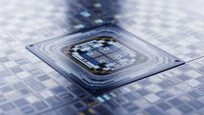
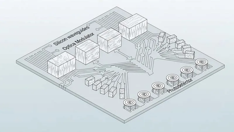
Silicon Photonics Integration Technology refers to the integration of optical functions on silicon substrates using CMOS-compatible manufacturing processes. Specifically, it enables modulators, waveguides, multiplexers, and photodetectors to be fabricated at wafer scale.
Unlike traditional approaches, this technology allows optical components to benefit from decades of semiconductor process optimization. Consequently, it achieves higher consistency, improved yield, and stronger scalability. More importantly, it creates a foundation for large-volume production that aligns with the needs of modern data infrastructure.
Why Silicon Photonics Has Become the Mainstream Platform
A Leap in Integration Density
First, Silicon Photonics Integration Technology dramatically increases integration density. By integrating multiple optical functions on a single chip, it reduces the number of discrete components and optical interconnections. As a result, optical modules become more compact and structurally simpler.
In addition, higher integration supports multi-channel architectures such as DR4 and FR4. Therefore, module designers can deliver higher port density within limited physical space. This advantage is critical for next-generation switches and servers.
Reshaping the Cost Structure
Equally important, Silicon Photonics Integration Technology fundamentally reshapes the cost model of optical modules. Traditional optical components often rely on specialized production lines, which limits scalability. In contrast, silicon photonics leverages mature CMOS fabs.
As production volumes increase, unit costs decline significantly. Consequently, high-speed optical modules become economically viable beyond core backbone networks. This cost efficiency accelerates adoption across metropolitan and access networks.
Manufacturing Consistency and Reliability
Furthermore, wafer-level fabrication ensures strong device uniformity. This consistency simplifies testing and calibration processes. Therefore, system reliability improves, and long-term operational stability becomes easier to guarantee.
Performance Impact on High-Speed Optical Modules
Supporting Higher Bandwidth Evolution
Silicon Photonics Integration Technology provides a scalable path toward higher transmission rates. By enabling parallel modulation and dense wavelength integration, it supports current 400G and 800G designs. Moreover, it prepares the industry for future 1.6T optical modules.
Because the architecture scales efficiently, designers can extend performance without redesigning the entire system. As a result, development cycles shorten and time-to-market improves.
Power Efficiency and Thermal Management
Another critical advantage lies in power efficiency. Silicon-based modulators exhibit favorable electro-optical performance. Therefore, overall module power consumption can be reduced.
However, higher integration also introduces thermal management challenges. For this reason, advanced packaging and heat dissipation designs play a crucial role. Nevertheless, the net efficiency gains remain significant for large-scale deployments.
Key Technical Challenges and Solutions
Laser Integration Constraints
Despite its advantages, Silicon Photonics Integration Technology faces inherent challenges. Most notably, silicon does not emit light efficiently. Therefore, external laser sources or heterogeneous integration techniques are required.
Currently, the industry adopts multiple approaches, including external laser sources and hybrid bonding. Each solution involves trade-offs among cost, reliability, and complexity. Nevertheless, ongoing innovation continues to improve feasibility.
Packaging and Testing Complexity
In addition, high-density integration raises packaging and testing requirements. Advanced optical packaging technologies are essential to unlock the full benefits of silicon photonics. Consequently, packaging capability has become a strategic differentiator in the value chain.
A System-Level View of the Silicon Photonics Ecosystem
From a broader perspective, Silicon Photonics Integration Technology is reshaping the entire optical communications ecosystem. Upstream, specialized silicon photonics foundries and design houses continue to mature. Meanwhile, optical module manufacturers are evolving toward system-level integration.
Downstream, cloud service providers and network operators benefit from lower cost per bit and improved reliability. Therefore, the technology delivers value across the entire industry chain.
Future Trends: Beyond Traditional Optical Modules
Looking ahead, Silicon Photonics Integration Technology will play a key role in emerging architectures. Co-Packaged Optics (CPO) represents one such direction, bringing optical interfaces closer to switching and computing chips.
Moreover, the combination of silicon photonics with advanced packaging and chiplet designs will further enhance system efficiency. As a result, optical interconnects will become more tightly integrated with computing platforms.
Practical Deployment and Industry Experience
As Silicon Photonics Integration Technology gains traction, proven system-level solutions become increasingly important. In this context, experienced solution providers help bridge advanced component technology and real-world network deployment.
HTF is one such company with deep expertise in optical communication systems. Backed by a team with more than ten years of experience in optical product development and fiber transmission solutions, HTF supports global data centers, 5G networks, cloud computing platforms, and metropolitan networks.
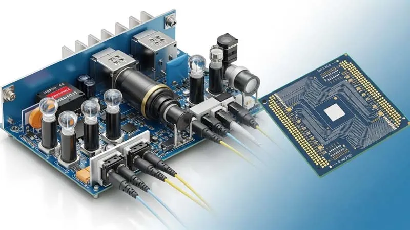
Its HT6000 OTN transmission system exemplifies practical innovation. Designed as a compact, high-capacity, and cost-efficient platform, HT6000 supports CWDM and DWDM architectures with flexible networking capabilities. Moreover, it meets node capacity requirements exceeding 1.6T, making it a highly cost-effective WDM expansion solution for IDC and ISP operators.

Conclusion: A Structural Shift in Optical Communications
In summary, Silicon Photonics Integration Technology is not merely an incremental improvement. Instead, it represents a structural shift in how optical modules are designed, manufactured, and deployed. By enabling high integration, lowering costs, and improving scalability, it aligns perfectly with the long-term evolution of global data infrastructure.
As networks continue to scale, this technology will remain central to high-end optical module development. At the same time, mature system solutions and experienced partners will play a vital role in translating technological potential into operational success.